 ve galyum nitrür (GAN) uygulamaları arasındaki fark nedir? - Vetek Yarıiletken")
 Kritik Değeri")


QR kod

Ürünler
Bize Ulaşın


Faks
+86-579-87223657

e-posta

Adres
Wangda Yolu, Ziyang Caddesi, Wuyi İlçesi, Jinhua Şehri, Zhejiang Eyaleti, Çin


Vetek Semiconductor, yarı iletken endüstrisi için önde gelen gözenekli SIC seramik üreticisidir. ISO9001 geçti, Vetek Semiconductor kalite üzerinde iyi bir kontrole sahiptir. Vetek Semiconductor her zaman gözenekli SIC seramik endüstrisinde yenilikçi ve lider olmaya kararlıdır.

Gözenekli sic seramik disk
Gözenekli SIC seramikleri, yüksek sıcaklıklarda ateşlenen ve içinde çok sayıda birbirine bağlı veya kapalı gözeneklere sahip seramik malzemedir. Aynı zamanda, gözenek boyutları 2 ila 100um arasında değişen mikro gözenekli vakum emme bardağı olarak da bilinir.
Gözenekli SIC seramikleri metalurji, kimya endüstrisi, çevre koruma, biyoloji, yarı iletken ve diğer alanlarda yaygın olarak kullanılmaktadır. Gözenekli SIC seramikleri köpükleme yöntemi, sol jel yöntemi, bant döküm yöntemi, katı sinterleme yöntemi ve emprenye piroliz yöntemi ile hazırlanabilir.

Sinterleme yöntemi ile gözenekli SIC seramiklerinin hazırlanması
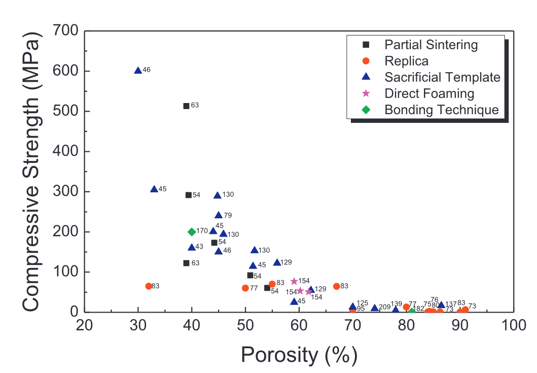
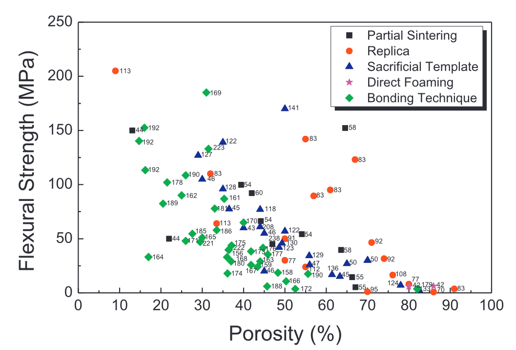
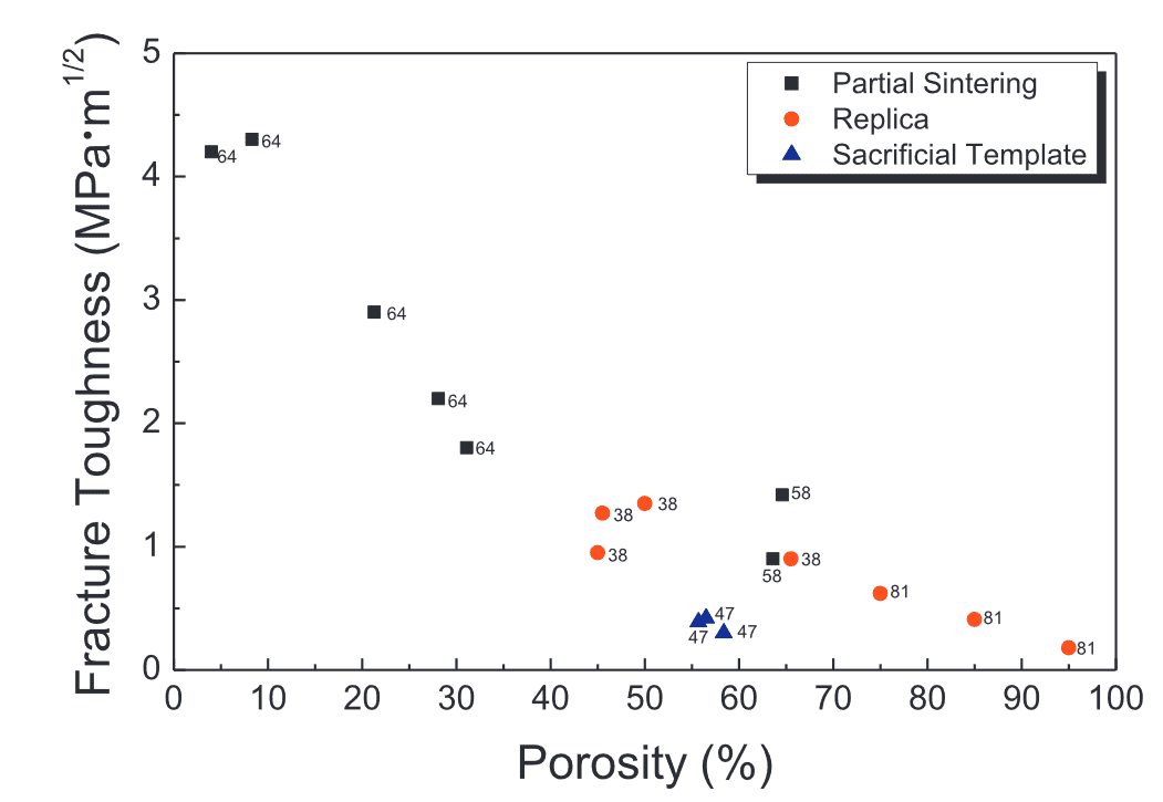
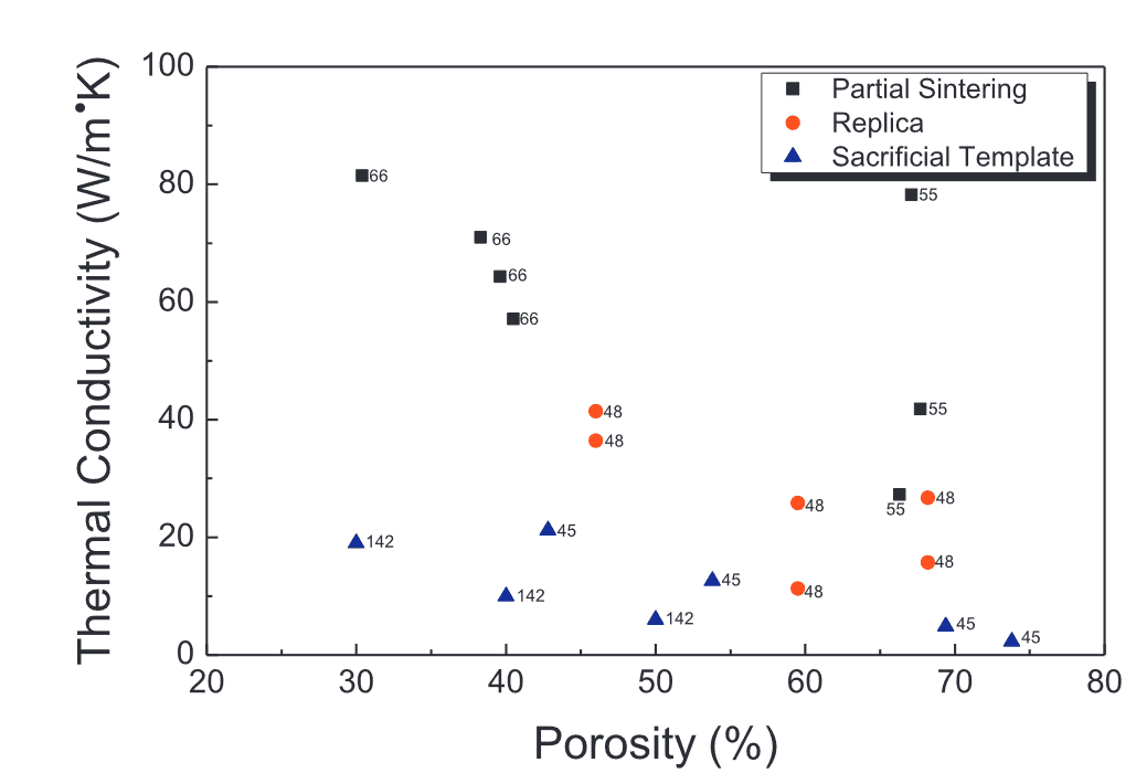
Gözenekli Silikon Karbür Seramiklerinin Özellikleri Gözenekliliğin bir fonksiyonu olarak farklı yöntemlerle hazırlanmıştır

Yarıiletken gofret imalatında gözenekli SIC seramik vantuzları
Vetek Semiconductor'ın gözenekli SIC seramikleri, yarı iletken üretiminde kelepçeleme ve taşıma taşıma rolünü oynar. Yoğun ve düzgün, mukavemet bakımından yüksek, hava geçirgenliğinde iyi ve adsorpsiyonda üniforma.
Gofret girintisi ve çip elektrostatik dökümü gibi birçok zor sorunu etkili bir şekilde ele alırlar ve aşırı yüksek kaliteli gofretlerin işlenmesine yardımcı olurlar.
Gözenekli SIC seramiklerinin çalışma diyagramı:

Gözenekli SIC seramiklerinin çalışma prensibi: Silikon gofret vakum adsorpsiyon prensibi ile sabitlenir. İşleme sırasında, gözenekli SIC seramikleri üzerindeki küçük delikler, silikon gofret ve seramik yüzey arasındaki havayı çıkarmak için kullanılır, böylece silikon gofret ve seramik yüzey düşük basınçta, böylece silikon gofret sabitlenir.
İşlemden sonra, silikon gofretin seramik yüzeye yapışmasını önlemek için plazma suyu deliklerden akar ve aynı zamanda silikon gofret ve seramik yüzey temizlenir.

Gözenekli SIC seramiklerinin mikro yapısı
Avantajları ve özellikleri vurgulayın:
● Yüksek sıcaklık direnci
● Aşınmaya karşı direnç
● Kimyasal direnç
● Yüksek mekanik mukavemet
● Yenilenmesi kolay
● Mükemmel termal şok direnci
öğe
birim
gözenekli sic seramikleri
Gözenek çapı
bir
10 ~ 30
Yoğunluk
g / cm3
1.2 ~ 1.3
Yüzey rouhung
bir
2.5 ~ 3
Hava emme değeri
KPA
-45
Bükülme mukavemeti
MPa
30 Dielektrik sabiti
1MHz
33 Termal iletkenlik
W/(m · k)
60 ~ 70
Gözenekli SIC seramikleri için birkaç yüksek gereksinim vardır:
1. Güçlü vakum adsorpsiyonu
2. Düzlük çok önemlidir, aksi takdirde operasyon sırasında sorunlar olacaktır
3. Deformasyon yok ve metal safsızlık yok
Bu nedenle, Vetek Semiconductor'ın gözenekli SIC seramiklerinin hava emilim değeri -45kPa'ya ulaşır. Aynı zamanda, safsızlıkları gidermek için fabrikadan ayrılmadan önce 1,5 saat boyunca 1200 ℃ 'de temperlenirler ve vakum torbalarında paketlenirler.
Gözenekli SIC seramikleri gofret işleme teknolojisinde, transfer ve diğer bağlantılarda yaygın olarak kullanılmaktadır. Bağlanma, kinasyon, montaj, parlatma ve diğer bağlantılarda büyük başarılar elde ettiler.


Order precision-engineered Porous SiC ceramics from Veteksemicon—ideal for thermal uniformity and gas control in semiconductor systems.
Veteksemicon’s porous silicon carbide (SiC) components are engineered for high-temperature plasma processes and advanced gas flow control. Ideal for PECVD, ALD, vacuum chucks, and gas distribution plates (showerheads), these components offer excellent thermal conductivity, thermal shock resistance, and chemical stability.
Our porous SiC features a controlled pore structure for consistent gas permeability and uniform temperature distribution, reducing defect rates and enhancing yield. It is widely used in wafer handling platforms, temperature equalizing plates, and vacuum holding systems. The material ensures mechanical durability under corrosive and high-load thermal conditions.
Contact Veteksemicon today to request custom Porous SiC solutions or detailed engineering parameters.
+86-579-87223657
Wangda Yolu, Ziyang Caddesi, Wuyi İlçesi, Jinhua Şehri, Zhejiang Eyaleti, Çin